
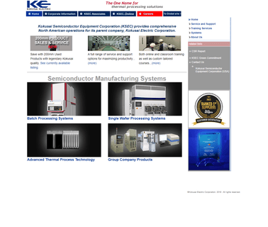
Thin Film, Dielectric Film Materials; Film Thickness, Uniformity Measurement, Ellipsometer; Process Equipment; Packaging & Assembly Materials; Inspection & Measurement Products; Deposition & Cvd, Pvd, Ald, Plating; Instruments, Bench Top Test; Thermal Processing ...
Semiconductor Components Assembly Equipment Industrial Valves Packaging and Cleaning Washing Pv Process Chemical Mechanical Polishing Etching Stripping Ashing Dry Wet Plating Electro Deposition Systems Chemicals Solids Acids Etchants Buffers Alkalis Bases Solvents Strippers Di Up Water Photo Resist Specility Layers Developers Ancillaries Surface Protection Material Coatings Materials Cmp Grind Lap Polish Abrasive Parts Accessories Flow Control Meters Gauges Regulators Mfcs Pipe Tubing Hose ...
Deposition Service; PV Services; Simulation, Analysis, Modeling Software; Research & Development; h, Strip, Cleaning Service; Failure Analysis, Analytical Services; Transfer Litho Masks, Polymer Masks, Nanoimprint Templates; Mask Making Software & Simulation; 304 Mask Making Materials ...
Packaging and Assembly Equipment; Plating, Electro Chemical Plating for device assembly; Process Equipment; Deposition, PVD, Sputtering, Evaporation Equipment; Plating, Electro Chemical Plating, Deposition Systems; Packaging and Assembly Materials; Thin Film, Dielectric Film Materials; Components, Parts & Accessories; Lamps (non Lithography), all type UV, LED Lamps for Lithography; Raw Material & Custom components, Metal; Sub systems; Exposure, Illumination Sources Laser, Lamp, X ray & other, Assembly Equipment, Lamp Parts ...
Chemical Electroplating Surface Treatment Processes, Electrolytic Deposition for Electroplating Technology, Multi Layer Composite Materials, Special Processes for Surface Treatment of Plastic Parts, Plastic Parts, Plastic Products ...

201 Flat Panel Display Equipment; Deposition, Pvd, Sputtering, Evaporation Equipment; Pcb, Wire Board & Pwb Test & Repair; Photolithography, Backplane, Color Filter & Tp; 307 Process Materials; Lithography & Exposure; Thermal Processing; Laser Treatment, Cutting Systems for Panels & Photocells; Process Equipment; Deposition & Target Materials ...
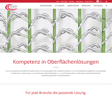
The Main focus of our work is on Electroplating. Our Fields of Activity Range from Developing new Layer Materials Together with the Necessary Deposition Processes and Process Chains, through Failure Analysis and right Up to Industrial Plants Engineering. Thus we can offer our Customers Support Throughout the Entire Development Process from the Initial Idea right Up to its ImplemenTation in Production. to Deliver this Wealth of Services, we Employ Staff from the Fields of Material Science, Chemistry, Surface Finishing ...
Process Equipment; Acids,hants; h, Strip, Cleaning Service; Packaging & Assembly Materials; Parts Cleaning, Micro Contamination; Process Materials; Ingots; Deposition, Pvd, Sputtering, Evaporation Equipment; Printing Masks, Screens; Reclaim Services ...

Equipment, Process; Solar Cell Substrates, Crystalline Silicon & C Si, Thin Film; PV Materials; Thin & Thick Film Substrates for Mems; Led; Deposition, Physical Vapor & Pvd, Sputtering, Evaporation Equipment; Ingots, Wafers; Oled Related Equipment & Materials, Panel & Module, Solar Cell ...

Thin Film, Thin Film Deposition, Thin Film Research, Sputtering Targets, Crucible Liners, E Beam Evaporation, Ebeam, E Beam, Crucible, E Beam Crucible, Starter Sources, Evaporation Materials, Plasma Spraying, Backing Plates, Metallic Bonding; Plasmaterials, Provides High Purity Deposition Materials In the Form of Sputtering Targets, Electron Beam Starter Sources, Evaporation Materials, Wire, and Many Other Forms for Nearly Every Element, Alloy, Composition, and Component On the Periodic Table, Optics Equipment, Photonics ...
for all your vacuum needs. KJLC is on the cutting edge of thin film technology and innovation, while offering unparalleled customer support. RD and batch production tools for the semiconductor industry and a wide variety of other applications. Automated vacuum systems for PVD and ALD, chambers, components, thin film deposition sources, and high purity materials. Other products offered: e beam sources, thermal, Semiconductor Industry, Building Equipment, HVAC Equipment ...

Flexible, configurable systems & leading edge processes; Oxford Instruments offers flexible, configurable process tools and leading edge processes for the precise, controllable and repeatable etching, deposition and growth of micro and nano structures. Our systems provide process solutions for the micro and nanometre engineering of materials for semiconductor, optoelectronics, HBLED, power devices, MEMS ...
Materials Processing Solutions, Wire Saw, Wheel Saw, Diamond Cut Off Saw, Diamond Wafering Saw, Cut Off Saw, Plasma Clean, Ion Mill, Ion Beam, Tripod Polishing, Sputter Deposition, Sputter Coat, Ion Etch, Ion Polish, Sample Mounting, Etching System, Acid Saw ...

Research, Development & Short Run Production of Vacuum Metallized Films & Thin Film Coatings, Involving Deposition on Substrate Materials & Pattern Coatings; Specialized Areas are Spacecraft Thermal Control Materials, Low Observable Materials & Electrical / Electronic Materials; Astral Technology Unlimited, Produces Thin Film Coatings and Vacuum Metalized Films for a variety of aerospace and communications applications ...
Thin Film, Dielectric Film Materials; Equipment, Process; Components, Parts; Heating Elements, Coils, Insulation, Vestibule Blocks, Furnace Components; Thin Film; Deposition, Chemical Vapor & Cvd, Mocvd, Pecvd, Lpcvd, Ald, Reald, Mvd; PV Equipment, Semiconductor Industry, Heating Components, Heating Elements ...