

Thanks for Visiting Silcotek Corporation; Silcotek Corporation Offers Custom, High Performance Silicon Coatings for Wafer Processing and Fabrication Applications; Silcotek's Cvd Coating Process Creates a Complete Internal and External Coating on Components with Simple to Complex Geometries. Ideal for all Gas Transfer Equipment Used in the Pv and Semiconductor Industries. If There is a Corrosion or Contamination Issue, use Silcotek Coatings to Lengthen Lifetimes and Reduce Defects; Improve Stainless, Semiconductor Industry ...
SPTS brings together over 40 years wafer processing experience and our industry leading solutions include silicon etch, dielectric etch, dry release etch, PVD, PECVD, MOCVD and MVD ...

Vistec, Electron, Beam, Nano, and, Biotechnology, Direct, Write, Mask, Making, Semiconductor, Patterning, Ebl, Nanolithographie, Nano, Lithography, Nems, Mems, Semiconductor, Elektronenstrahl, 200Mm, 300Mm, Silicon, Photonics, Metrology, Calibration, Electron, Gun, Hologram, Wasserzeichen, Gitter, Direct, Write, Mask, Write, Wafer, Clean, Room, Reinraum ...
Fire Fighting Equipment Safety Industrial Research Development Semiconductor Microelectronics Industry Wafer Foundry Bipolar High Voltage Dielectic Isolated Thin Film Active Passive Components Flip Chip Sensor Technologies Inertial Pressure Temperature Gas Smoke Detectors Optoelectronic Discrete Integrated Circuits Diffused Light Wave Guides Mach Zender Modulators Epitaxy Diffusion Oxidation Ion Implant Lpcvd Pecvd Platinum Silicidation Photolithography Plasma Etching Silicon Micromachining Koh Anisotropic Etch Sputter Deposition Resistor Lift Off ...

100Mm Silicon Wafers, 125Mm Silicon Wafers, 4 Inch Silicon Wafers, Wafer Processing, Silicon Wafer Processing, Wafer Services, Silicon Wafer Services, Oxide Wafers, Epitaxial Wafers, Si, Si, Silicon Test Wafers, Silicon ...
P Type Solar Grade Silicon Wafer, Silicon Ingot, Silicon Wafer, Silicon Polished Wafer, Mono Silicon, Solar Grade Silicon Wafer, 156156Mm Solar Silicon Wafer for Solar Cell ...
Solar Cell, Diodes, LED, Compound Wafer, Silicon Epi Wafer, Silicon Wafer, Solar Wafer, Silicon Wafer Processing, LED Gaas Wafer, LED Sapphire Wafer, Solar Cell, Transistors and Diodes ...

Thermal Oxide Service, Silicon Nitride Service, 300Mm Processing Service, Wafer Processing, 300Mm, 200Mm, Silicon Wafers, Silicon Wafer Processing, 300Mm Processing, Wafer Processing Services; Thermal Oxide, Silicon Nitride, Peteos Oxide, Photomasking Services, 300Mm Processing, 200Mm Processing, Photolithography Service, 200Mm Oxide, 300Mm Oxide, Lpcvd Nitride, Silicon, Silicon Wafers, 300Mm Wafers, Standards, Nist Traceable, Nist Traceable Standards; Thin Film Standards, Sio2 Standards, Silicon ...

Polishing Pad, Polishing Slurry, Sapphire Polishing Pad, Sapphire Polishing Slussy, Silicon Wafer Polishing ...

Mems, Market, Sensor, Sensors, Consulting, Marketing, Study, Report, Survey, Microsystem, Microtechnology, Microtechnologies, I, Micronews, Micronews, Nano, Microelectronics, Semiconductor, Led, Oled, Ic, Moems, Optoelectronic, Cmos, Inertial, Imu, Gyro, Accelero, Biomems, Biochip, Microfluidic, Compound, Silicon, Wafer, Soi, Sic, Si, Gan, Rf, Semiconductor Industry ...
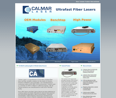
Solar Cell, Ps Laser, Femtosecond Laser, Fs, Fiber, Picosecond Laser, Ultrafast, Calmar, Cazadero, Mendocino, Eureka, Coronado, Amplitude, Coherent, Ophthalmology, Scribing, Spectroscopy, Ablation, Photovoltaic, Pulsed, Micromachining, Solar Cell, Sapphire, Led, Thin Film, Arc Ablation, Antireflective Coating Ablation, Silicon Wafer Scribing, Gaas, Faser Laser, Femtosekunden Laser, Laser Materialbearbeitung, Pikosekunden Laser, Solarzellen Laser, Kurzpuls Ablation, Photovoltaik Laser, Ablation Nicht Reflektierender ...

MicroSense Precision Wafer Measurement Systems; MicroSense UltraMap – the New Standard for 200mm Polished Wafer Flatness Measurement; the new MicroSense UMA C200L wafer metrology system measures the flatness, thickness and shape of bare 200mm silicon wafers with industry leading throughtput, 32% higher than legacy systems. the UltraMap system provides; Industry standard dual capacitance sensor measurement ...
EXPERTISE IN WET ETCHING & CLEANING EQUIPMENT; Global Zeus, established in 1970, has been growing alongside the semiconductor industry for more than 48 years. We provide wet etching and cleaning equipment and technologies. Our market leading wet station and single spin processor are widely used for photoresist stripping, silicon nitride etching, metal etching, and wafer cleaning and contain higher throughput ...

Monocrystalline Silicon Solar Panel (80S), Solar Ingots, Solar Wafer, Solar Cell, Solar Module, Solar Panel, Solar Integrated System, Solar Cell ...

Integrated Circuits, Asic, Ic, Analog, Asic Design, Mixed Signal, Digital, Design, Layout, Test, Semiconductor, Cmos, Wafer, Die, Silicon, Integrated, Circuit, Application Specific, D/A, A/D, Prototype, Soic, Tssop, Package, Chip Scale, Chip, Amplifier, Comparator, Sensor, Telecom, Medical; Low Power Turnkey Asic Design Services Specializing in Analog Asic & Mixed Signal Asic Design & Production; Low power turnkey ASIC design services specializing in analog ASIC & mixed signal ASIC design & production ...
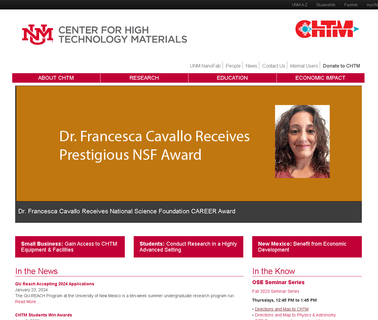
Iii V Multi Layer Epitaxial Wafer Production Services. Public Access to Cleanrooms & Process Tools. the Center for High Technology Materials is a 60,000 Square Foot Research Facility at the University of new Mexico. We have two Cleanrooms Open to the Public which offer a full Suite of Semiconductor Process Tools for Fabricating State Of The Art Iii V, Silicon, Glass, Heterogeneous Materials and Devices for Photonic, Laser, Optical Communication; Applications. as a State Funded Faciliity, we, Optics Equipment, Photonics ...