

Enterprise-class network monitoring and server monitoring solutions. network topology maps, alerting and reporting tools. monitor availability and performance of your hosts ...
Packaging and Assembly Equipment; Litho for WLP: Bumping, D Interconnect Aligners; Inspection & Measurement Products; Defect, Particle, Contam. Detection, Review, Inspect; Die Inspection, Die Shear; Film Thickness, Uniformity Measurement, Ellipsometer; Line Width, Critical Dimension (CD) Measurement; Microscopes: Confocal Scanning, D Video; Microscopes: Optical Microscopes; Overlay Measurement; Metrology, Topology, Nanotopography, Flatness, Cryst.Orient; Test Equipment; Probe Card Maintenance, Semiconductor Components, Assembly Equipment ...

Inspection & Measurement Products; Chromatograph; Film Thickness, Uniformity Measurement, Ellipsometer; Flat, Notch Finding System; Instruments, Bench Top Test; Leak Detection Systems Vacuum or Gas; Microscopes: Atomic Force Microscopes (AFM); Particle Monitors, Analyzers Airborne or Liquid; Plate Inspection Equipment; Spectrometers, FTIR, ATR FTIR, Auger Electron (AES), SIMS; Stress, Refractive Index, Reflectivity, Conductivity Meas; Metrology, Topology, Nanotopography, Flatness, Cryst.Orient, Semiconductor Industry ...
Packaging and Assembly Equipment; Backgrind, Slicing, Lapping, Polishing Equipment; Dicing, Sawing, Scribing, Separation Equipment; Wafer Level Bonders; Wafer Mount, Taping Equipment; Cutting, Drilling, Laser ablation, Beveling Equipment; Vacuum drying & out gassing Systems; Inspection & Measurement Products; Instruments, Bench Top Test; Metrology, Topology, Nanotopography, Flatness, Cryst.Orient; MEMS Equipment; Wafer Level Bonders; PV Equipment; Wafers; Thin Film; Process Equipment; Chemical, Semiconductor Components, Assembly Equipment ...
Microscopes; Optical Microscopes; Die Inspection, Die Shear; Thermal Sensing, Measurement, Analysis; Wafer, Substrate Metrology, Topology, Nanotopography, Flatness Measurement, Crystalline Orientation; Defect, Particle, Bump, Contamination Detection, Review or Inspection; Line Width, Critical Dimension & Cd Measurement; Inspection & Measurement ...
Semiconductor Industry Welding Machine Equipment Assembly Ball Placement Attach Systems Dicing Sawing Scribing Separation Die Bonding Sorter Pick and Place Flip Chip Dispensing Solder Reflow Soldering Brazing Wafer Level Bonders Wire General Use Inspection Measurement Shear Substrate Metrology Topology Nanotopography Flatness Crystalline Orientation Test Pv Wafers Burn Accessory Discrete Component Materials Adhesives Epoxi ...

Equipment, Test; Wafer, Substrate Metrology, Topology, Nanotopography, Flatness Measurement, Crystalline Orientation; Probing Equipment Incl. Analytical, Circuit, Manual, E Beam, Optical, Wafer Probers; Microscopes; Scanning Electron Microscope & Sem, Focused Ion Beam & Fib, Transmission Electron Micr; Equipment, Nanotechnology; Inspection & Measurement, Semiconductor Industry ...

Inspection & Measurement Products; Metrology, Topology, Nanotopography, Flatness, Cryst.Orient; PV Equipment; Wafers; Process Equipment; Wafer Identification, Marking Equipment; Mask Making Materials; Mask plate blanks, Glass; PV Materials; Ingots, Wafers; Process Materials; Quartzware, Ceramic & Oxide Ceramic Fixtures; Substrates; Prime, Polished, Mirrored Wafers; Thin & Thick film substrates for MEMS; Sub-systems; Optics, Lens Products, Auto-Focus Systems ...
Inspection & Measurement Products; Metrology, Topology, Nanotopography, Flatness, Cryst.Orient; Production Control Software; Die Inspection, Die Shear; Test Programs; Wire Bonding Inspection, Test; Pv Equipment; Defect, Particle, Contam. Detection & Review & Inspect; Line Width, Critical Dimension & Cd Measurement; Yield Mgmt, Process Control Software ...

Wafer Handling; Inspection & Measurement Products; Metrology, Topology, Nanotopography, Flatness, Cryst.Orient; Software Programming, Software Development; Instruments, Bench Top Test; Test Services or Consulting; Test Equipment; Analytical Probe Stations & Instruments, Equipment, Accessories; Microanalysis & Digital Imaging Systems for Materials Analysis; Products; Surface Analysis Systems; Image Analysis Systems ...
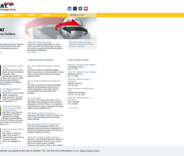
EtherCAT sets new standards for real time performance and topology flexibility, while meeting or undercutting traditional fieldbus cost levels. EtherCAT features include high precision device synchronization, cable redundancy options, and a functional safety protocol SIL3. EtherCAT is an international standard IEC, ISO and SEMI. In addition, EtherCAT P is a new breakthrough technology that adds the option, Semiconductor Industry, Networking Cable ...
Inspection & Measurement; Optical Measuring Systems; Machining; Machine Controls; Inspection & Measurement; Noncontact Measurement Systems; Inspection & Measurement; Probes; Mold Components; Fixtures; Inspection & Measurement; Wafer, Substrate Metrology, Topology, Nanotopography, Flatness Measurement, Crystalline Orientation; Film Thickness, Thickness, Uniformity Measurement, Ellipsometer; Data Collection, Building, Assembly Equipment, Injection Mould, Die Casting ...
Inspection & Measurement Products; CV (capacitance-to-voltage) Probe systems; Film Thickness, Uniformity Measurement, Ellipsometer; Resistivity Measurement; point probe, Sheet resistance; Stress, Refractive Index, Reflectivity, Conductivity Meas; Metrology, Topology, Nanotopography, Flatness, Cryst.Orient; PV Equipment; Inspection and Metrology ...
Equipment, Inspection & Measurement; CV (capacitance-to-voltage) Probe systems; Defect, Particle, Bump, Contamination Detection, Review or Inspection; Die Inspection, Die Shear; Film Thickness, Thickness, Uniformity Measurement, Ellipsometer; Microscopes: Optical Microscopes; Plate Inspection Equipment; Resistivity Measurement, 4 point probe, Sheet resistance; Stress, Refractive Index, Reflectivity & Conductivity Measurement; Wafer, Substrate Metrology, Topology, Nanotopography, Flatness Measurement ...
3D Skin Imaging and Diagnostic Solutions. In Vivo High Performances Systems Dedicated to Non Contact 3D Measurements of the Skin Topography, Face Topology, Body Topometry. Beside the 3D Measurements, Eotech Provides High Resolution Echography, and Thermal Imaging Instruments. They are Used to Evaluate Cosmetics and Dermatological Products and Treatments Efficacy, Mainly for Anti Ageing Effects, Beauty Products, Cosmetics ...
Packaging & Assembly Equipment; Overlay Measurement; Sub Systems; Litho for Wlp; Bumping, 3D Interconnect Aligners; Gas, Liquid Delivery Panels As Subsystems; Metrology, Topology, Nanotopography, Flatness, Cryst.Orient; Nanotechnology Equipment & Tools; Cleaning, Washing Equipment for Assembly & Packaging; Inspection & Measurement Products; Plasma Sources, Controls, Monitoring, Diagnosis, Assembly Equipment ...