
E+H Metrology Offers a Complete Line of Wafer Geometry, Resistivity and Stress Measurement Systems. Wafers Up to 450Mm can be Measured on Manual Gauges or Fully-Automated Robotic or Belt Sorters Using Advanced Software. Thickness, Flatness, Bow, Warp, Stress and Wafer Resistivity can all be Measured in a Single High-Throughput Wafer Sorter Using the Advanced E+H Mx-Nt Operating Software. E+H's Proprietary Waferstudio Offers Unique 3D Visualization and Analysis. the E+H Manual Gauges and Automated ...
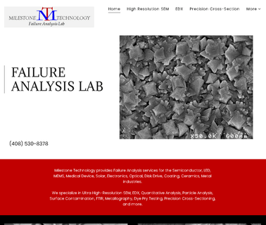
Failure Analysis Lab, Cross Section, Edx, Particle Analysis, Coatings, Ultra High Resolution Sem, Edx Analysis, Tsvs, Vias, Bumps, Wafer Contamination, Cross Section, Printed Circuit Boards, Ftir Analysis, Failure Analysis, Bga Inspection; Precision Cross Sectionand Failure Analysis Lab. SEM, EDX, Mapping, Quantitative Analysis, Cross Section Services, Semiconductor Industry ...
Microscopes; Optical Microscopes; Die Inspection, Die Shear; Thermal Sensing, Measurement, Analysis; Wafer, Substrate Metrology, Topology, Nanotopography, Flatness Measurement, Crystalline Orientation; Defect, Particle, Bump, Contamination Detection, Review or Inspection; Line Width, Critical Dimension & Cd Measurement; Inspection & Measurement ...

Packaging and Assembly Equipment; Litho for WLP: Bumping, D Interconnect Aligners; Wafer Level Bonders; Wafer Mount, Taping Equipment; Flat Panel Display Equipment; Luminous Layer Patterning and Sealing Equipment; Seal Patterning Equipment; Inspection & Measurement Products; Thermal Sensing, Measurement, Analysis; Metrology, Topology, Nanotopography, Flatness, Cryst.Orient; MEMS Equipment; Wafer Level Bonders; PV Equipment; Wafers; Thin Film; Process Equipment; Wafer Identification, Marking Equipment, Assembly Equipment ...
Semiconductor Industry Welding Machine Assembly Equipment Packaging and Deflashing Degating Tools Dicing Sawing Scribing Separation Marking Imprinting Labeling Molding Encapsulation Decapsulation Printing Equip Screen Alignment Film Flat Panel Display Laser Treatment Cutting Systems Panels Photocells Scribe Break Drilling Ablation Beveling Pv Wafers Modules Thin Integration Automation Process Wafer Identification Test Failure Analysis ...

Wafer Handling; Inspection & Measurement Products; Metrology, Topology, Nanotopography, Flatness, Cryst.Orient; Software Programming, Software Development; Instruments, Bench Top Test; Test Services or Consulting; Test Equipment; Analytical Probe Stations & Instruments, Equipment, Accessories; Microanalysis & Digital Imaging Systems for Materials Analysis; Products; Surface Analysis Systems; Image Analysis Systems ...

Plasma Etch, Plasmaetch, Plasma Cleaning, Plasma Cleaner, Decapsulation, Ic Decapsulation, Failure Analysis, Ic Counterfeit Detection, Plasma Surface Treatment, Rie, Reactive Ion Etch, Hybrid Assembly, Wire Bonding, Wafer Bonding, Resist Strip, Descum, Wafer Bump Reflow, Passivation Removal, Probe Card Cleaning, Contact Angle Meter, Goniometer, Solar Cell Edge Etching, Ild Removal, Surface Energy, Dlc Wafer Reclaim, Solder Reflow, Rapid Thermal Annealing, Hybrid Packaging, Void Free Solder, Bench Top, Solar Cell ...

Test Equipment; Burn In Systems; Circuit Repair, Design Mod, Memory Repair, Mask Repair Sys; Probe Card Maintenance and Analysis Systems; Probing: Analytical, Circuit, Manual, E Beam, Optical, Wafer; Test Materials; Boards: Burn In, Performance (Low, High Temp and Ceramic); Probe Cards, DUT boards probing accessories; Test Sockets, Contactors and Contact accessories, Simulation Training, Electronic Plugs ...
Equipment, Assembly; Instruments, Bench Top Test; Test Services or Consulting; Equipment, General Use; PV Systems; Equipment, Test; Failure Analysis Systems; Wafer Mount, Taping Equipment; Repair, Rework Equipment; Measurement & Control Technology, Semiconductor Industry ...

Come explore our wafer and board level probing solutions. Micromanipulator provides the best probing solutions for failure analysis, product development, characterization, and system level test available in the industry. We specialize in probing applications for both wafer level and decapsulated board mounted IC's, offering wafer and board solutions with above and below ambient temperature stress technologies. Our, Industrial Computer ...

Probing Equipment Incl. Analytical, Circuit, Manual, E Beam, Optical, Wafer Probers; Equipment, Test; System On a Chip & Soc, Mixed Signal Test Systems; Probe Card Maintenance & Analysis Systems; Memory Test Systems ...

Sonoscan Provides Reliable Non Destructive Analysis for Process Control and Quality Assurance Utilizing Non Immersion Techniques to Safeguard your Products as it Accurately Detects Defects and Process Variations. Sonoscan has the Latest Products in our full Line of Instruments for the Laboratory, as well as Automated Test Systems for Front, Mid and back End Microelectronics. Starting with the C Sam Aw Series for Various Wafer Configurations and the Next Generation Facts 2 Model Df2400 for Scanning, Printed Boards ...