

Wafer Processing, Wafer Services, Silicon Wafer Services, Oxide Wafers, Epitaxial Wafers, Si, Si, Silicon Test Wafers, Silicon Prime Wafers, Sio, Sio, Silicon Test Slices, Virginia Semiconductor, Electronic Parts ...
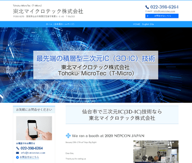
Tohoku Microtec is Provider of 2.5/3D Stacking Ic Service; Tohoku Microtec is a Partner and Technical Representative of Giniti. Ginti is the Leading Edge Ic Process Facility Started by Tohoku University to Provide Fabrication Services to Worldwide Clients that are Interested in Developing new 2.5D/3D Integration Technologies; Using the Base Technology Originally Developed at Tohoku University in Japan we offer a Broad Range of 2.5/3D Ic Services Including; Prototype Processing by Wafer On Chip Using, Semiconductor Industry ...

Coat, Develop, Resist Processing, Track; Fpd Color Filter Materials; Equipment; Systems Materials, Chemicals; Surface Protection Material, Coatings; Aligners Equipment; Materials; Solids Cleaning Chemicals, Solvents; Strippers Dopants, Liquid Or; Assembly; Lithography Systems for Wafer Level Packaging, Bumping, 3D Interconnect; Process, Semiconductor Industry ...

Equipment, Process; hing, Stripping, Ashing Dry & Wet Equipment; Coat, Develop, Resist Processing, Track Equipment; Thermal Processing Diffusion, Oxidation, Annealing, Rta, Rtp Equipment; Mems Equipment; Dispensing Systems; Wafer Level Bonders; Probing; Analytical, Circuit, Manual, E Beam, Optical, Wafer; Packaging & Assembly Equipment; Alignment Film Coating Equipment; Thermal Processing; Litho for Wlp; Bumping, 3D, Semiconductor Components, Assembly Equipment ...

Thanks for Visiting Silcotek Corporation; Silcotek Corporation Offers Custom, High Performance Silicon Coatings for Wafer Processing and Fabrication Applications; Silcotek's Cvd Coating Process Creates a Complete Internal and External Coating on Components with Simple to Complex Geometries. Ideal for all Gas Transfer Equipment Used in the Pv and Semiconductor Industries. If There is a Corrosion or Contamination Issue, use Silcotek Coatings to Lengthen Lifetimes and Reduce Defects; Improve Stainless, Semiconductor Industry ...

Semiconductor Industry Welding Machine Heating Components Elements Assembly Equipment Building Hvac Electrical Circuits Packaging and Die Bonding Attach Molding Encapsulation Decapsulation Wire Process Thermal Processing Materials Interface Heat Sinks Parts Accessories Chucks Wafer Substrates Furnace Sub Systems Temp Sensing Control Recirculators Chillers Exch ...

Roducts; Cleaning System; Single Wafer Cleaner: Su-3300, Su -3200, Su-3100; Spin Scrubber: Ss-3200, Ss-3100; Wet Station: Fc-3100, Fc-821L, Ws-620C/Ws-820L; Resist Processing System; Coat/Develop Track Dt-3000 Rf-310A Sk-60Ex/80Ex; Frontier Project; Single Wafer Cleaner Su-2000; Spin Scrubber Ss-80Ex; Compact Wet Station Cw-1500; Spray Coater Sc-80Wx; Wafer Pattern Inspection System Zi-2000; Direct Imaging System for Advanced Packaging Dw-3000; Annealing System; Flash Lamp Annealer La-3000-F; Laser ...

Lasers, Laser Systems, Uv, Ultraviolet, Solid State, Co2, Diode Laser, Hene Laser, Ion Lasers, Coherent, Spectra Physics, Newport, Omnichrome, Jds Uniphase, American Lasers, Ilt, Laser Physics, Confocal Microscopy, Cytometry, Dna, Dvd Mastering, Flow Cytometry, Facsdiva, Facs Diva, Metrology, Etec, Applied Materials, Spectroscopy, Holography, Innova Fred, Innova 300, Sabre, Innova, Wafer Inspection, Lithography, Mask Processing, Molecular Spectroscopy, Raman Spectroscopy, Semiconductor, Argon; Gas-ion ...

Copper Interconnect, Strain Engineering, Ald, Chemical Vapor Deposition, Flat Panel Display, Etch, Rapid Thermal Processing, Pvd, Dielectric, Epitaxial, Polysilicon, Wafer Defect Inspect, Chemical Products, Industrial Computer ...
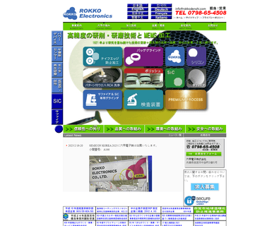
Continue to strive for leading the semiconductor production; Introduction of the original process `ROKKO puremium process` turned to the visitor troubled by knife edge or the cleanning factor on the back of a pattern (particle and contamination) while thinning processing of the wafer for power and sensors progressed, Back grind ojf 6 inch SiC and sapphire wafer, polish(CMP), proposal of washing technology, Semiconductor Industry ...

Mems, Micro, and, Nano, Electronic, Equipment, Semiconductor, Coating, Process, Wet, Process, Equipment, Substrate, Cleaning, Etching, Lift, Off, Single, Wafer, Cover, Chuck, Processor, Post, Cmp, Cleaning, Coating, Developing, Wafer, Substrate, Lithography, Photoresist, Wet, Processing, Spin, Coater, Spray, Coater, Ebr, Temporary ...
Wet process solutions for the semiconductor industry. Single wafer processing, batch processing, etching, cleaning, wafer, plating, ECD, eless plating, panel ...