

Wafer Processing, Wafer Services, Silicon Wafer Services, Oxide Wafers, Epitaxial Wafers, Si, Si, Silicon Test Wafers, Silicon Prime Wafers, Sio, Sio, Silicon Test Slices, Virginia Semiconductor, Electronic Parts ...

Packaging and Assembly Equipment; Backgrind, Slicing, Lapping, Polishing Equipment; Cleaning, Washing Equipment for Assembly & Packaging; Dicing, Sawing, Scribing, Separation Equipment; Die Bonding, Attach Equipment; Die Removal Equipment; Die Sorter, Pick & Place; Flip Chip Placement Systems; Wafer Level Bonders; Wafer Mount, Taping Equipment; Repair, Rework Equipment; Inspection & Measurement Products; Defect, Particle, Contam. Detection, Review, Inspect; MEMS Equipment; Wafer Level Bonders; Process, Assembly Equipment ...
Packaging and Assembly Equipment; Backgrind, Slicing, Lapping, Polishing Equipment; Dicing, Sawing, Scribing, Separation Equipment; Wafer Level Bonders; Wafer Mount, Taping Equipment; Cutting, Drilling, Laser ablation, Beveling Equipment; Vacuum drying & out gassing Systems; Inspection & Measurement Products; Instruments, Bench Top Test; Metrology, Topology, Nanotopography, Flatness, Cryst.Orient; MEMS Equipment; Wafer Level Bonders; PV Equipment; Wafers; Thin Film; Process Equipment; Chemical, Semiconductor Components, Assembly Equipment ...
Tohoku Microtec is Provider of 2.5/3D Stacking Ic Service; Tohoku Microtec is a Partner and Technical Representative of Giniti. Ginti is the Leading Edge Ic Process Facility Started by Tohoku University to Provide Fabrication Services to Worldwide Clients that are Interested in Developing new 2.5D/3D Integration Technologies; Using the Base Technology Originally Developed at Tohoku University in Japan we offer a Broad Range of 2.5/3D Ic Services Including; Prototype Processing by Wafer On Chip Using, Semiconductor Industry ...
Flat Panel Display Equipment; Laser Treatment, Cutting Systems for Panels & Photocells; Cutting, Drilling, Laser ablation, Beveling Equipment; MEMS Equipment; Wafer Level Bonders; Process Equipment; Wafer Identification, Marking Equipment, Semiconductor Industry ...
Coat, Develop, Resist Processing, Track; Fpd Color Filter Materials; Equipment; Systems Materials, Chemicals; Surface Protection Material, Coatings; Aligners Equipment; Materials; Solids Cleaning Chemicals, Solvents; Strippers Dopants, Liquid Or; Assembly; Lithography Systems for Wafer Level Packaging, Bumping, 3D Interconnect; Process, Semiconductor Industry ...
our ebooth portal. E+H Metrology offers a complete l ine of Wafer Geometry, Resistivity and Stress measurement systems. Wafers up to 450mm can be measured on manual gauges or fully automated robotic or belt sorters using advanced software. Thickness, Flatness, Bow, Warp, Stress and wafer Resistivity can all be measured in a single high throughput wafer sorter using the advanced E+H MX NT operating software. E+H's, Semiconductor Industry, Sports Accessories ...
Mpi Corporation, LED, Mpi Corporation, Probe Cards, Wafer Probe Cards, Thermal Test, Probe Stations, LED Test, Semiconductor Test, Probe Stations, Wafer Probing Solutions, Wafer Probing, Led; 19957Led Mpi Corporation Mpi Led ...
Bearings, Shaft Collars; Flow Control Components Valves, Meters, Gauges, Regulators, Mfc's; Sensors; Components, Parts; Gaskets, Seals, ORings, Elastomers, Resins; Chucks for Wafer, Substrates; Pipe, Tubing, Hose, Flanges, Connectors, Couplings, Plumbing Fittings, Semiconductor Industry, Bearings, Automotive Parts ...
Diffusion Furnace Chambers for wafer fabrication. Our offerings of standard gauge chambers, from 400 degC 1350 degC, Low Mass & Fast Ramp Chambers temperature ranges from 200 degC 1250 degC Speciality chmabers to 1750 degC are available. We also provide Direct Replacement Horizontal and Vertical heaters for TEL & Kokusai & ASM & Aviza & SVG Thermco & Centrotherm, as well as Torch elements, Vestibule Blocks and Soft, Semiconductor Industry ...

Brooks robot repair, Brooks robots, Brooks robot, Mag7, PRI/equipe, PRI/equipe robot, PRI/equiperobot repair, used equipment, used robot, used robots, Brooks cluster tool, Brooks Automation cluster tool, vacuum cassette elevator, semiconductor robot, used semiconductor robot, spare robot parts, Equipe robot, Equipe robot parts, Equipe robot part, Equipe pre aligner, Equipe pre aligner repair, wafer handling, wafer handling robot, used wafer handling robot; Maintenance and Repair Services ...

Vistec, Electron, Beam, Nano, and, Biotechnology, Direct, Write, Mask, Making, Semiconductor, Patterning, Ebl, Nanolithographie, Nano, Lithography, Nems, Mems, Semiconductor, Elektronenstrahl, 200Mm, 300Mm, Silicon, Photonics, Metrology, Calibration, Electron, Gun, Hologram, Wasserzeichen, Gitter, Direct, Write, Mask, Write, Wafer, Clean, Room, Reinraum ...
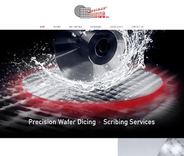
Production Facility for Semiconductor and Microelectronics Industry. Services Include Wafer Dicing, Die Sorting, Die Bonding and Wirebonding; Ceramic Dicing Service; Dicing ...

Fiber Optics, Electronic Connectors, Semiconductor Wafer Polishing, Metallographic, Metallography, Fiber Optic Connectors, Data Storage, Precision Optics, Advanced Ceramics, Corrosion Inhibitors, Lapping, Polishing, Nanofinish Corporation; Finishing Equipment; Precision surface finishing for semiconductors, fiber optics, hard drives, precision optics and engineering ceramics by NANOFINISH Corporation; Precision Surface Finishing For Semiconductors, Fiber Optics, Hard Drives, Precision Optics & Engineering Ceramics ...

Equipment, Semiconductor, Microelectronics, Wafer, Furnace, Diffusion, Qxidation, LPCVD, RTP, Solar Cell, III V Epitaxy, Environmental Analytical systems, Annealing, APCVD, Brazing, Chemisorption, Complete abatement management, Consulting & project planning, Soldering Tools, Industrial Equipment, Solar Cell ...
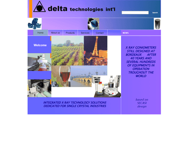
Delta Technologies, Secasi Goniometer, X Ray Goniometer, Crystal Orientation, Wafer Measurement; Cutting Services; Machining; Slicing Services; integrated x ray solutions for singal crystal industries; Semiconductor Cutting, Ceramic Machining Service ...